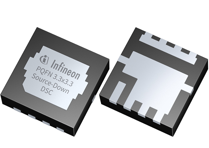
The design of future power electronics systems will continue to advance to achieve the highest level of performance and power density. In response to this trend, Infineon Technologies has introduced a new 3.3 x 3.3 mm2 PQFN package with a source base power MOSFET in the voltage range of 25-150 V and available in bottom cooling (BSC) and double-sided cooling (DSC) configurations.
The new product family delivers significant performance improvements at the semiconductor device level, offers an attractive solution for DC-DC power conversion, and opens up new possibilities for system innovation in server, communications, OR-ing, battery protection, power tools, and charger applications.
The new product family uses Infineon's latest MOSFET product technology and leading packaging technology to bring system performance to new levels. Inside the source base (SD) package, the source contacts of the MOSFET wafer are flipped and oriented toward the plantar side of the package, then welded to the PCB. In addition, the package has an improved drain copper clip design inside the top of the chip, achieving a market-leading chip/package area ratio.
As the size of the system continues to shrink, the two key factors of reducing power loss and improving heat dissipation become critical. Infineon's new line of products offers a 25% reduction in on-going resistance (RDS(on) compared to the current market leader PQFN 3.3x 3.3mm ² drain-bottom package. Infineon Double-sided heat dissipation, PQFN package, OptiMOS™ source base power mosFeTs provide an enhanced thermal interface that conducts power losses from switching devices to radiators. The double-sided cooling structure can connect the power switch to the heat sink in the most direct way, and its power consumption capacity is three times higher than that of the bottom-cooling, bottom-source power MOSFET.
The new product family offers two different pin arrangement forms, providing great flexibility for PCB wiring. The pin arrangement of traditional standard gate layout can be used to modify the existing drain base design quickly and simply. The pin arrangement of gate centered layout provides a new possibility for multiple devices to be connected in parallel, and can minimize the line distance between the driver chip and gate. The new generation 25-150 V OptiMOS™ source bottom-power mosFeTs in PQFN 3.3x 3.3mm ² package deliver superior continuous current capability up to 298A for the highest system performance.
The Products You May Be Interested In
 |
CAR2512FPBC5-Z01A | AC/DC CONVERTER 12V 2500W | 287 More on Order |
 |
CCR0512FPXXXZ01A | AC/DC CONVERTER 12V 500W | 348 More on Order |
 |
AXH010A0D93-SR | DC DC CONVERTER 2V 20W | 495 More on Order |
 |
AXH010A0F-SRZ | DC DC CONVERTER 3.3V 33W | 255 More on Order |
 |
EVK011A0B41-HZ | DC DC CONVERTER 12V 132W | 117 More on Order |
 |
ESTW004A2C41-SZ | DC DC CONVERTER 15V 63W | 110 More on Order |
 |
QRW025A0A71-H | DC DC CONVERTER 5V 125W | 133 More on Order |
 |
HW006A6A1-SZ | DC DC CONVERTER 5V 30W | 417 More on Order |
 |
QW050A1 | DC DC CONVERTER 5V 50W | 125 More on Order |
 |
QHW100A71 | DC DC CONVERTER 5V 100W | 178 More on Order |
 |
JW150H1 | DC DC CONVERTER 24V 150W | 398 More on Order |
 |
JHW050FG | DC DC CONVERTER 3.3V 2.5V 50W | 228 More on Order |
 |
HW025FG | DC DC CONVERTER 3.3V 2.5V 25W | 241 More on Order |
 |
DC025ACL-M | DC DC CONVERTER 5V +/-15V 25W | 117 More on Order |
 |
AXA003A0X-SR | DC DC CONVERTER 0.8-5.5V 16W | 436 More on Order |
 |
ATA006A0X4 | DC DC CONVERTER 0.8-5.5V 33W | 483 More on Order |
 |
AXH003A0X | DC DC CONVERTER 0.8-3.6V 10W | 293 More on Order |
 |
AXA003A0X4 | DC DC CONVERTER 0.8-5.5V 16W | 367 More on Order |
 |
AXA003A0X | DC DC CONVERTER 0.8-5.5V 16W | 214 More on Order |
 |
JNCW016A0R64-18Z | DC DC CONVERTER 28V 448W | 120 More on Order |
 |
EHHD006A0B841-HZ | DC DC CONVERTER 12V 72W | 139 More on Order |
 |
SHHD005A0F41-SRZ | DC DC CONVERTER 3.3V 15W | 307 More on Order |
 |
PDT012A0X43-SRZ | DC DC CONVERTER 0.45-5.5V | 352 More on Order |
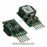 |
NSR010A0X4Z | DC DC CONVERTER 0.6-6V 60W | 1246 More on Order |

 Semiconductors


 Passive Components


 Sensors


 Power
Power


 Optoelectronics


