Semiconductor packaging technology is a key part of the chip manufacturing process, which directly affects the performance, reliability and cost of integrated circuits. Among them, Panel Level Packaging (PLP) technology, as an emerging high-density packaging solution, is gradually becoming the focus of the industry. Samsung Electronics and Taiwan Semiconductor Manufacturing Company (TSMC), as the two giants of the global semiconductor industry, have launched fierce competition and technology exploration in this field.
Overview of PLP technology
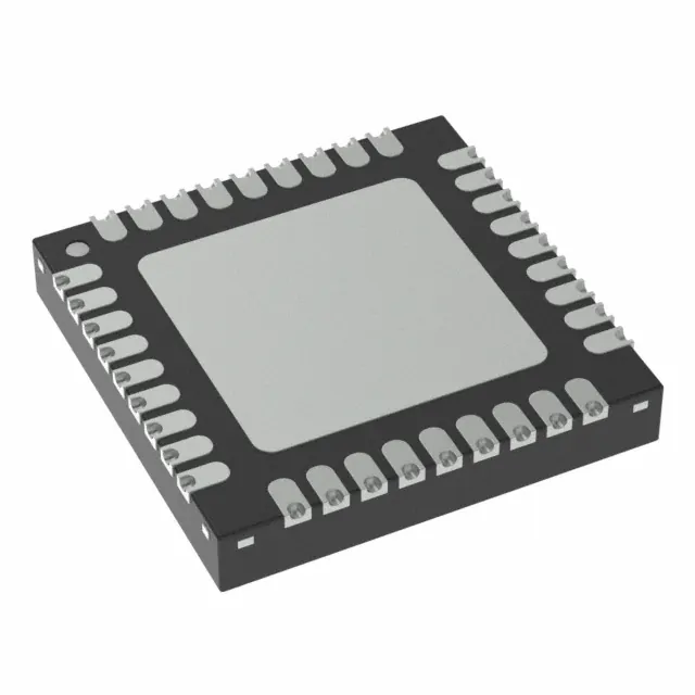
PLP is a panel-based Packaging technology that has significant advantages in packaging efficiency and cost control compared to traditional wafer-based packaging technologies (such as WLP, Wafer Level Packaging). PLP technology arranges multiple BZX84C5V6-7-F chips on a large panel for packaging, which can not only improve production efficiency, but also reduce material waste. In addition, PLP technology can also achieve higher integration and smaller package sizes to meet the needs of modern electronic devices for miniaturization and high performance.
Samsung Electronics' lead
Samsung Electronics started early in PLP technology, showing a significant first-mover advantage. Its PLP technologies, such as FOPLP (Fan-Out Panel Level Packaging), significantly improve production efficiency and reduce costs by packaging directly at the chip level on large panels rather than traditional wafer-level or small-size panels. This technology enables smaller line-widths/pitches, increased package density, and support for multi-chip packages (MCP), making it ideal for high-performance computing, mobile devices, and iot applications.
Through continuous investment in research and development, Samsung has optimized materials, processes and equipment to solve the challenges of low yield and thermal management in the early stage of PLP technology. For example, it developed eXtended FOPLP (XFOP) technology to further improve package integration and performance, providing powerful support for high-end smartphone and data center applications.
Challenges and solutions of TSMC
In the face of Samsung Electronics' leading position in the PLP field, TSMC has adopted an aggressive strategy to catch up. Although TSMC's traditional strength lies in wafer foundry, it has also shown strong research and development strength and market adaptability in advanced packaging technology. TSMC's integrated fan-out package (InFO) technology, while not a typical PLP, lays a solid foundation for subsequent entry into the PLP market.
In order to narrow the gap with Samsung in PLP technology, TSMC has accelerated the development and commercialization of PLP-related technologies. TSMC's PLP solutions focus on improving production efficiency, reducing costs, and meeting customer needs for high performance, low power consumption, and miniaturization. By working closely with upstream and downstream partners in the industry chain, TSMC continuously optimizes panel size, material selection and process control to improve yield and reduce costs, thereby maintaining an edge over the competition.
Conclusion
With the continuous progress of semiconductor packaging technology, PLP technology, as a new packaging solution, has shown broad application prospects. With its technology accumulation, vertically integrated production model and marketing strategy, Samsung Electronics has achieved a leading edge in the field of PLP technology. TSMC, as a global semiconductor foundry giant, although facing challenges in PLP technology, by strengthening research and development investment, optimizing the supply chain, and developing an effective market strategy, TSMC is expected to catch up, achieve technological breakthroughs and increase market share.
In the future, the competition of PLP technology is not only the competition of technical strength, but also the competition of market strategy and customer relationship. In this process, technological innovation and production efficiency will become the key factors for enterprises to win. With the continuous development of PLP technology, we have reason to expect that future electronic devices will be more miniaturized and high-performance, bringing more convenience and surprises to people's lives.
The Products You May Be Interested In
 |
3845 | 3X4 MATRIX KEYPAD | 419 More on Order |
 |
473 | SWITCH PUSHBUTTON SPST-NO RED | 350 More on Order |
 |
1187 | SWITCH PUSHBUTTON SPST-NO WHT | 489 More on Order |
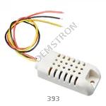 |
393 | SENSOR HUMID/TEMP 5V DTL 2% MOD | 950 More on Order |
 |
3238 | 802.3AF POE OUTPUT DATA & POWER | 251 More on Order |
 |
628 | STARTER PK EL PANEL 10X10CM WHT | 222 More on Order |
 |
2554 | DIGITAL RGB LED WEATHERPROOF STR | 360 More on Order |
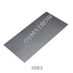 |
3803 | ADDRESS LED 64X32 FLEX RGB MATRX | 262 More on Order |
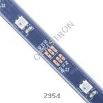 |
2954 | ADDRESS LED STRIP SERIAL RGB 5M | 103 More on Order |
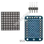 |
959 | ADDRESS LED MATRIX I2C BLUE | 244 More on Order |
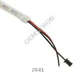 |
2841 | ADDRESS LED STRIP SERIAL RGBW 1M | 550 More on Order |
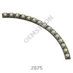 |
2875 | ADDRESS LED RING 1/4 SER RGBW | 247 More on Order |
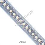 |
2848 | ADDRESS LED STRIP SERIAL RGBW 1M | 244 More on Order |
 |
3630 | ADDRESS LED STRIP RGBW | 325 More on Order |
 |
2862 | ADDRESS LED RING SERIAL RGBW | 456 More on Order |
 |
2970 | ADDRESS LED STRIP SERIAL RGB 1M | 320 More on Order |
 |
1768 | ADDRESS LED RING 1/4 SERIAL RGB | 686 More on Order |
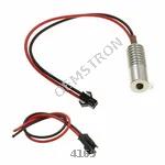 |
4169 | FIBER OPTIC LIGHT SOURCE 1W PINK | 240 More on Order |
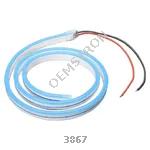 |
3867 | FLEXIBLE SILICONE NEON-LIKE LED | 371 More on Order |
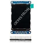 |
1480 | 2.2 COLOR TFT LCD DISP W/MICROSD | 626 More on Order |
 |
326 | DISPL OLED GRAPHIC MONO 128X64 | 490 More on Order |
 |
398 | RGB BACKLIGHT POSITIVE LCD | 397 More on Order |
 |
1856 | SMALL 1.2 8X8 BRIGHT SQUARE PURE | 293 More on Order |
 |
1378 | WS2811 LED DRIVER CHIP - 10 PACK | 360 More on Order |

 Semiconductors


 Passive Components


 Sensors


 Power
Power


 Optoelectronics


